The race to build faster AI systems is running into a quiet constraint: packaging. It’s no longer just about designing powerful chips. The real slowdown is happening after the silicon is made, when those chips are stitched together into a working system.
That’s the problem an Australian startup is stepping into.
Syenta said Tuesday it has raised $26 million in Series A funding to bring a new manufacturing method to market, one that could ease persistent supply chain pressure tied to artificial intelligence. The round was led by Playground Global and Australia’s National Reconstruction Fund, with participation from Investible, Salus Ventures, Jelix Ventures, and Wollemi Capital. The latest raise brings the company’s total funding to A$51.1 million (US$36.4 million), signaling continued backing as it moves toward commercialization.
The company plans to open a U.S. office in Arizona, placing itself near major fabrication hubs run by Intel and Taiwan Semiconductor Manufacturing Company. Former Intel CEO Pat Gelsinger, now a general partner at Playground Global, will join Syenta’s board as part of the deal.
The timing reflects a shift happening across the semiconductor industry. AI chips from players like Nvidia and Google are no longer single pieces of silicon. They’re built from multiple chiplets that need to be connected with high precision using advanced packaging. That step, led largely by TSMC, has turned into one of the biggest chokepoints in the AI supply chain.
“Today’s advanced packaging approaches have real limits on interconnect density, which constrain the bandwidth between chips,” said Dr. Jekaterina Viktorova, CEO and founder of Syenta. “We’re enabling finer-pitch connections within existing manufacturing infrastructure, allowing systems to move more data more efficiently and at a lower cost without requiring entirely new fabrication approaches.”
This Startup Thinks It Can Fix AI’s Biggest Chip Bottleneck: Syenta Raises $26M and Brings in Pat Gelsinger
Inside Syenta’s pitch is a simple observation: the constraint is no longer compute alone. Interconnects and packaging are now setting the pace.
Today’s process relies on a base layer that functions almost like a giant chip. Building it takes time and drives up cost, slowing how quickly companies can scale production.
Syenta’s approach flips that model. Instead of constructing the base layer through traditional fabrication, the company uses an electrochemical process that acts more like stamping copper wiring directly onto it. The method cuts the number of steps by about 40% and avoids the need for specialized manufacturing tools. More importantly, it shortens production time from hours to minutes.
“This process takes minutes, as opposed to several hours, so it’s a massive difference in how you build your copper interconnects,” CEO and co-founder Jekaterina Viktorova said in an interview.
The speed gain doesn’t just improve output. It changes the math of the supply chain. Faster base layer production means more chips can move through the system, easing one of the hidden bottlenecks behind AI growth.
Gelsinger sees broader implications. In his view, the technology could reshape how chipmakers think about scaling advanced designs at a time when packaging limits are becoming more visible than raw compute gains.
“You open up a much bigger, more standardized, more available supply chain, yet with the density and performance” gains that drove chipmakers toward such complex designs in the first place, Gelsinger said.
Syenta is already working with several chip designers and is targeting high-volume production by 2028.
What the company is betting on is straightforward: fixing packaging could unlock more progress than squeezing incremental gains out of chip design itself. If that plays out, the next leap in AI performance may come from how chips are connected, not just how they’re built.
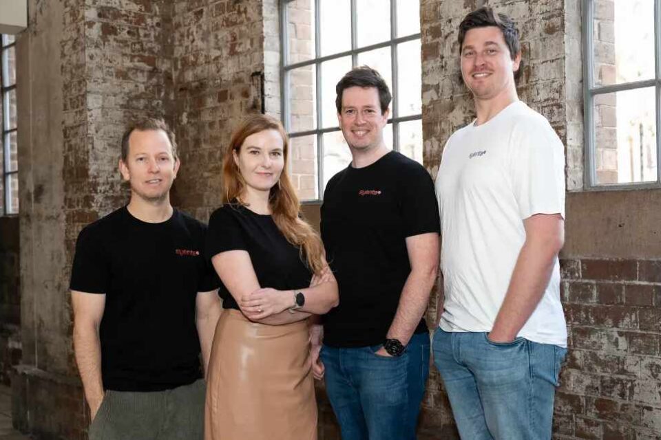
Co-founders of Syenta; Dr. Jekaterina Viktorova, CEO and Ben Wilkinson, CTO